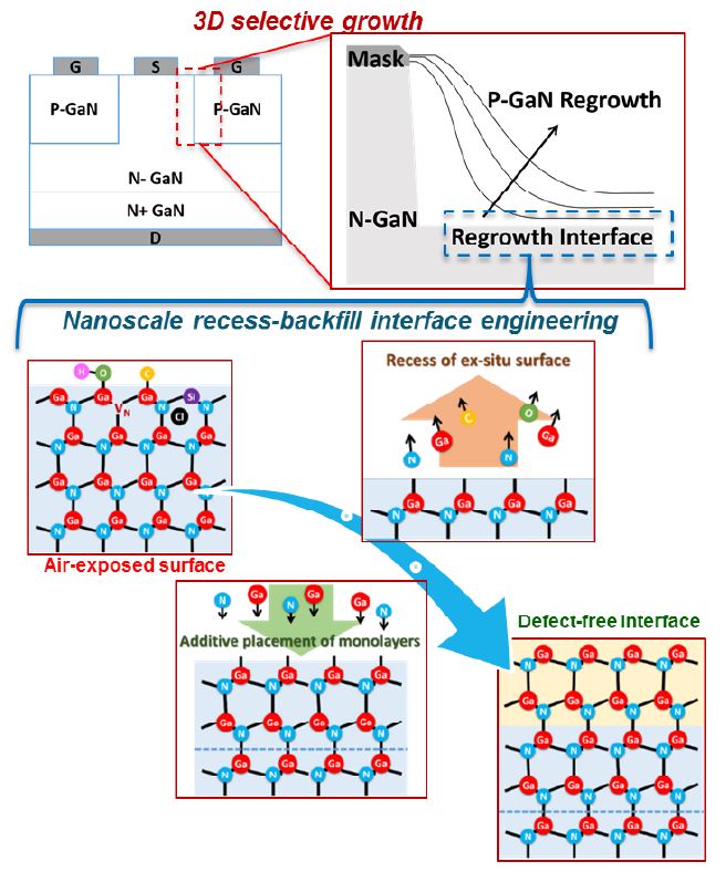
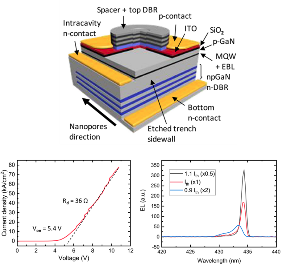
Han's research group works on interdisciplinary topics in electrical engineering, applied physics, material science, and surface chemistry. We investigate the epitaxial science and applications of III-nitride materials. In the past decade, III-nitride materials have enabled crucial technologies such as energy-efficient solid-state illumination and next-generation power electronics.


Blue VCSELs

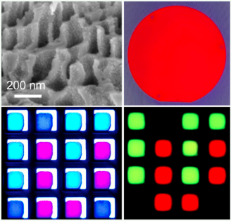
We have developed a novel conductivity based selective electrochemical etching to introduce nanometer sized pores into GaN. By controlling the doping and electrochemical etching bias, we are able to control the pore morphology. The nanoporous (NP) GaN can be considered a new form of GaN with an unprecedented tunability in optical index. We show the potential of this NP-GaN to overcome the optical and epitaxial limitations of AlGaN, which has been the bottleneck for GaN-based laser diodes for decades. The advantage of NP-GaN for vertical surface-emitting laser diodes (VCSELs) is that NP-GaN works as low refractive index material that is lattice-matched to GaN. We successfully demonstrated room-temperature pulse-operation of blue NP VCSELs under electrical injection.


Selective area growth and doping for power electronics

Gallium Nitride (GaN)-based electronic devices have attracted considerable attentions due to its wide bandgap, large critical electric field and high electron mobility. In order to achieve the theoretical performance of GaN power devices, it is needed to develop selective area doping (SAD) technique of either p- or n-type to enable design flexibility and create lateral PN junction devices as a building block for high-power devices. Unlike silicon (Si) or silicon carbide (SiC), in which lateral junctions can be achieved by ion-implantation and dopant diffusion processes, GaN cannot be easily doped by these two techniques. Alternatively, selective-area etching (SAE) followed by selective-area growth (SAG) are being explored as a possible solution to overcome this obstacle.

Cl-based plasma etching or dry etching of GaN is widely used to create trenches and patterns of a high aspect ratio and side walls with smoothness and verticality. However, plasma-induced damage introduces serious optical and electrical deteriorations. Recently, we introduced a metal-organic (MO) precursor, tertiarybutylchloride (TBCl), into MOCVD system for GaN to remove the plasma-induced damage or replace the role of plasma etching.

Wafer-scale transferrable LD for PIC

Photonic integrated circuits (PICs) have received much attention due to their applications in multiple fields such as signal processing and data transmission. However, they are limited by the materials that create them: typically, those materials can only build poor light emitters. Since its first demonstration in 1996, the GaN laser diode became the most outstanding light source in the blue wavelength range.

We explore the possibility of hetero-integration of blue laser diode to the PICs, which would introduce an efficient pumping light source with high output power. Edge-emitting laser diodes was first fabricated on the wafer with facets formed by dry etching and wet polishing. Using the concept of electropolishing, blue laser bars will be lifted-off and transfer to PICs in the wafer-scale.


NPQD Micro-LED

The micro-LED technology is of great interet to industries for the next-generation high-resolution display (applications like AR/VR). Difficulties are encountered with mass transfer when it comes to either the pick-and-place accuracy and the efficiency of LED with small dimension. Down conversion of the pumping photon energy (blue) through colloidal quantum dots to red and green is the approach we took. We embeded green or red quantum dots in scattering media, which is porous GaN. Near-unity light conversion efficiency (>97%) was realized for planarly loaded wafers. We also fabricated small pixels with red and green QDs loaded.