MOCVD and CVD Synthesis

A dedicated commercial MOCVD system (Aixtron 200/4 RF) is used for the growth of AlGaInN materials for optoelectronics, microelectronics, and nanosynthesis. The reactor is equipped with six metalorganic precursors and three hydride sources. A hot wall, flow-tube reactor is used for the synthesis of GaN nanowires and CVD-polymerization of conjugated organic semiconductors.


Optoelectronic Characterization


Multiple cryogenic and high magnetic field facilities exist in the lab. UV photoluminescence setup with laser excitation at 263nm (from a frequency-quadrupled solid state source) and 325 nm (HeCd laser). Variable-temperature probe station (MMR) setup for I-V, electroluminescence, and optical power measurement. Variable temperature Hall measurement is available for transport measurement.


Material Characterization


Multiple device characterization laboratories exist, including a dedicated MOS characterization lab with a wide assortment of probe stations, semiconductor parameter analyzers, and techniques (I/G/C-V, DLTS) are available. Nanoscale structures are probed by FTIR Spectrometer (Nicolet Nexus 870), NSOM System, field-emission SEM, High-resolution transmission electron microscopy (TEM) and electron diffraction (ED) (FEI Tecnai 20 Field Emission TEM at Trinity College, JEOL 200 at Yale Medical School), scanning energy dispersive x-ray spectrometry (EDS) (Philips CM-12 TEM.), A triple-axis x-ray diffractometer (Bede D-1) is available for microstructural analysis.


Yale School of Engineering & Applied Science Cleanroom (shared)


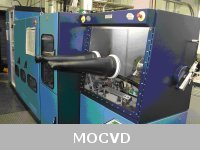
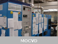
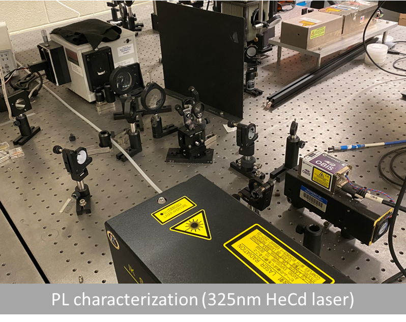
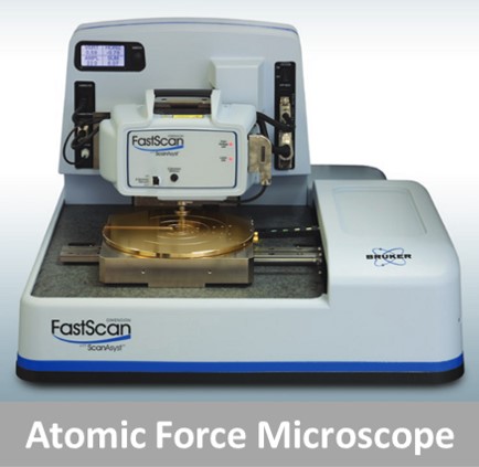
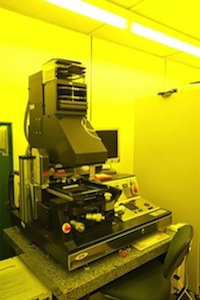
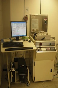
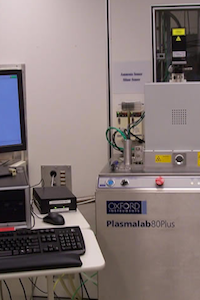
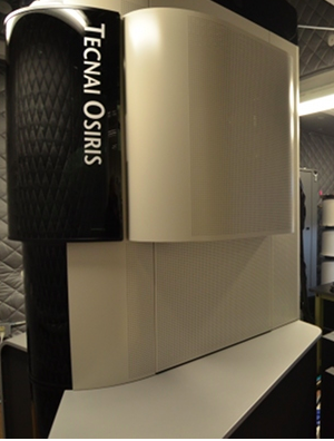
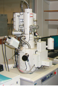
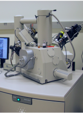
Full microelectronic processing facilities exist, including multiple vacuum evaporators, process furnaces, standard photolithography and wet chemical processing, PECVD, 2 Oxford reactive ion etchers (one fluorine-based and one ICP for chlorine-based), and fabrication characterization in a shared-use class 100/1000 cleanroom complex occupying a 3000 sq-ft contiguous area, for both silicon and III-V semiconductor processing. On site characterization includes inspection SEMs, EDX, AFM.

The SEAS Cleanroom is a Core science facility which is administrated by the School of Engineering & Applied Science (SEAS), and is under the directorate of the Office of the Provost. It is located on the fifth floor of the Becton Engineering and Applied Science Center at 15 Prospect Street. The Cleanroom is operated as an internal service provider to the Yale community, and recovers some of its operating costs through user fees and access fees.

Today the SEAS Cleanroom serves over 90 graduate students, research associates, and post doctoral associates, and supports research in Electrical Engineering, Applied Physics, Mechanical Engineering, Biomedical Engineering, Cell Biology, and Physics. There are currently three full time staff members consisting of a Cleanroom Director and two technicians, who are responsible for training new users, maintenance and repair of equipment and facilities, and to provide process engineering consultation and technical assistance as requested.


Yale Institute for Nanoscience and Quantum Engineering (shared)


The Yale Institute for Nanoscience and Quantum Engineering (YINQE) is a new initiative at Yale University intended to develop collaborations among disparate scientific disciplines centered on nanoscale research projects. YINQE builds on existing research strengths in engineering, and the physical and life sciences to broaden the interdisciplinary activity among faculty and students across the entire campus. Several dozen Yale faculty are already involved with YINQE, and more will be joining.

YINQE has characterization equipment including: 1 Transmission Electron Microscopy - The FEI Tecnai Osiris 200kV TEM; 2 Scanning Electron Microscopy - The Hitachi SU-70 and the The FEI XL40; 2 Atomic Force Microscopy - The The Bruker (Digital Instruments) Dimension 5000 and another Bruker (Digital Instruments) multimode AFM with a 1 cm sample stage. YINQE also possesses fabrication tools such as: Vistec EBPG 5000+ electron-beam lithography system, a dual-beam Focused Ion Beam (FIB)system, KLA Tencor Alphastep profilometer et cetera.

The core areas of our initial focus are: electronics, photonics, biomedical technology, nanoparticle synthesis, interfacial chemistry and quantum engineering. To enhance interdisciplinary research and stimulate new research opportunities that the Institute can enable, the Institute will administer and fund seed research projects, and will facilitate and coordinate interdisciplinary research proposals to external funding agencies.