Judy J. Cha's Google Scholar Link
Publications before Yale (2006 - 2014) --
51. |
Optical transmission enhancement through chemically tuned two-dimensional bismuth chalcogenide nanoplates J. Yao, K. J. Koski, W. Luo, J. J. Cha, L. Hu, D. Kong, V. Narasimhan, K. Huo, Y. Cui Nature Communications 5:5670 doi:10.1038/ncomms6670 (2014)
|
50. |
Improving lithium-sulphur batteries through spatial control of sulphur species deposition on a hybrid electrode surface H. Yao, G. Zheng, P.C. Hsu, D. Kong, J. J. Cha, W. Li, Z. W. Seh, M. T. McDowell, K. Yan, Z. Liang, V. K. Narasimhan, Y. Cui Nature Communications 5:3943 doi:10.1038/ncomms4943 (2014)
|
49. |
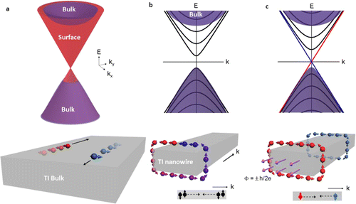
One-dimensional helical transport in topological insulator nanowire interferometers S. S. Hong, Y. Zhang, J. J. Cha, X.-L. Qi, Y. Cui Nano Letters 14, p.2815-2821 (2014)
|
48. |
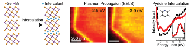
Two dimensional chalcogenide nanoplates as tunable metamaterials via chemical intercalation J. J. Cha, K. J. Koski, K. C. Y. Huang, K. X. Wang, W. Luo, D. Kong, Z. Yu, S. Fan, M. L. Brongersma, Y. Cui Nano Letters 13, p.5913-5918 (2013)
|
47. |
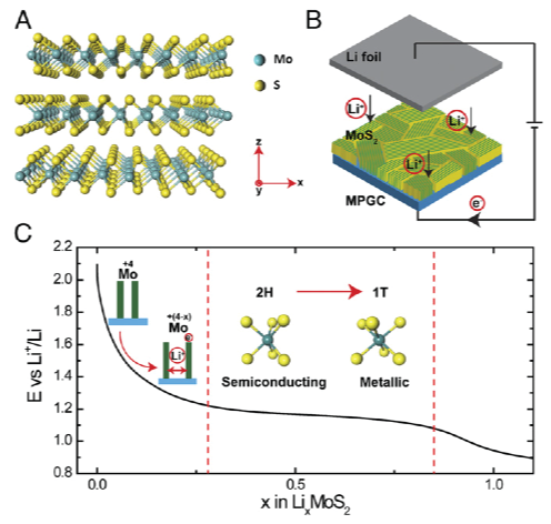
Electrochemical tuning of vertically aligned MoS2 nanofilms and its applications in improving hydrogen evolution reaction H. Wang, Z. Lu, S. Xu, D. Kong, J. J. Cha, G. Zheng, P.-C. Hsu, K. Yan, D. Bradshaw, F. B. Prinz, Y. Cui Proceedings of National Academy of Sciences 110, p.19701-19706 (2013)
|
46. |
First-row transition metal dichalcogenide catalysts for hydrogen evolution reaction D. Kong, J. J. Cha, H. Wang, H. R. Lee, Y. Cui Energy & Environmental Science 6, p.3553-3558 (2013)
|
45. |
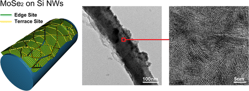
MoSe2 and WSe2 nanofilms with vertically aligned molecular layers on curved and rough surfaces H. Wang, D. Kong, P. Johanes, J. J. Cha, G. Zheng, N. Liu, Y. Cui Nano Letters 13, p.3426-3433 (2013)
|
44. |
Amphiphilic surface modification of hollow carbon nanofibers for improving the cycle life of lithium sulfur batteries G. Zheng, Q. Zhang, J. J. Cha, Y. Yang, W. Li, Z. Seh, Y. Cui Nano Letters 13, p. 1265-1270 (2013)
|
43. |
Synthesis of MoS2 and MoSe2 films with vertically aligned layers D. Kong, H. Wang, J. J. Cha, M. Pasta, K. J. Koski, J. Yao, Y. Cui Nano Letters 13, p. 1341-1347 (2013)
|
42. |
Ambipolar field effect in Sb-doped Bi2Se3 nanoplates by solvothermal synthesis D. Kong, K. J. Koski, J. J. Cha, S. S. Hong, Y. Cui Nano Letters 13, p. 632-636 (2013)
|
41. |
Sulfur-TiO2 yolk-shell nanoarchitecture with internal void space for long-cycle lithium-sulfur batteries Z. W. Seh, W. Li, J. J. Cha, G. Zheng, Y. Yang, M. T. McDowell, P.-C. Hsu, Y. Cui Nature Communications 4:1331 doi:10.1038/ncomms2327 (2013)
|
40. |
Topological insulator nanostructures J. J. Cha, K. J. Koski, Y. Cui physica status solidi – Rapid Research Letters DOI 10.1002/pssr.201206393 (2012), invited review article
|
39. |
Effects of magnetic doping on weak antilocalization in narrow Bi2Se3 nanoribbons J. J. Cha, M. Claassen, D. Kong, S. S. Hong, K. J. Koski, X.-L. Qi, Y. Cui Nano Letters 12, p.4355-4359 (2012)
|
38. |
The surface surfaces J. J. Cha, Y. Cui Nature Nanotechnology 7, p. 85-86 (2012), News&Views article
|
37. |
Weak antilocalization in Bi2(SexTe1-x)3 nanoribbons and nanoplates J. J. Cha, D. Kong, S. S. Hong, J. G. Analytis, K. Lai, Y. Cui Nano Letters 12, p.1107-1111 (2012)
|
36. |
Chemical intercalation of zero-valent metals into 2D layered Bi2Se3 nanoribbons K. J. Koski, C. D. Wessells, B. W. Reed, J. J. Cha, D. Kong, Y. Cui Journal of the American Chemical Society 134, 13773-13779 (2012)
|
35. |
Ultra-low carrier concentration and surface-dominant transport in antimony-doped Bi2Se3 topological insulator nanoribbons S. S. Hong, J. J. Cha, D. Kong, Y. Cui Nature Communications 3:757 doi:10.1038/ncomms1771 (2012)
|
34. |
High-density chemical intercalation of zero-valent copper into Bi2Se3 nanoribbons K. J. Koski, J. J. Cha, B. W. Reed, C. D. Wessells, D. Kong, Y. Cui Journal of the American Chemical Society 134, p.7584-7587 (2012)
|
33. |
High-mobility field-effect transistors from large-area solution-grown aligned C60 single crystals H. Li, B. C-K. Tee, J. J. Cha, Y. Cui, J. W. Chung, S. Y. Lee, Z. Bao Journal of the American Chemical Society 134, p.2760-2765 (2012)
|
32. |
Self-limited plasmonic welding of silver nanowire junctions E. C. Garnett, W. Cai, J. J. Cha, F. Mahmood, S. T. Connor, M. G. Christoforo, Y. Cui, M. D. McGehee, M. L. Brongersma Nature Materials 11, p.241-249 (2012)
|
31. |
Functionalization of silicon nanowire surfaces with metal-organic frameworks N. Liu, Y. Yao, J. J. Cha, M. T. McDowell, Y. Han, Y. Cui Nano Research 5, p.109-116 (2012)
|
30. |
Rapid surface oxidation as a source of surface degradation factor for Bi2Se3 D. Kong*, J. J. Cha*, K. Lai, H. Peng, J. G. Analytis, S. Meister, Y. Chen, H.-J. Zhang, I. R. Fisher, Z.-X. Shen, Y. Cui (*equal contribution) ACS Nano 5, p.4698-4703 (2011)
|
29. |
Improving the performance of lithium-sulfur batteries by conductive polymer coating Y. Yang, G. Yu, J. J. Cha, H. Wu, M. Vosgueritchian, Y. Yao, Z. Bao, Y. Cui ACS Nano 5, p.9187-9193 (2011)
|
28. |
Highly conductive, mechanically robust, and electrochemically inactive TiC/C nanofiber scaffold for high-performance silicon anode batteries Y. Yao, K. Huo, L. Hu, N. Liu, J. J. Cha, M. T. McDowell, P. K. Chu, Y. Cui ACS Nano 5, p.8346-8351 (2011)
|
27. |
Hollow carbon nanofiber-encapsulated sulfur cathodes for high specific capacity rechargeable lithium batteries G. Zheng, Y. Yang, J. J. Cha, S. S. Hong, Y. Cui Nano Letters 11, p.4462-4467 (2011)
|
26. |
Ambipolar field effect in the ternary topological insulator (BixSb1-x)2Te3 by composition tuning D. Kong, Y. Chen, J. J. Cha, Q. Zhang, J. G. Analytis, K. Lai, Z. Liu, S. S. Hong, K. J. Koski, S.-K. Mo, Z. Hussain, I. R. Fisher, Z.-X. Shen, Y. Cui Nature Nanotechnology 6, p.705-709 (2011)
|
25. |
Nano-structured textiles as high-performance aqueous cathodes for microbial fuel cells X. Xie, M. Pasta, L. Hu, Y. Yang, J. McDonough, J. Cha, C. S. Criddle, Y. Cui Energy & Environmental Science 4, p.1293-1297 (2011)
|
24. |
Low reflectivity and high flexibility of tin-doped indium oxide nanofiber transparent electrodes H. Wu, L. Hu, T. Carney, Z. Ruan, D. Kong, Z. Yu, Y. Yao, J. J. Cha, J. Zhu, S. Fan, Y. Cui Journal of the American Chemical Society 133, p.27-29 (2011)
|
23. |
In situ transmission electron microscopy observation of nanostructural changes in phase-change memory S. Meister, S. Kim, J. J. Cha, H.-S. P. Wong, Y. Cui ACS Nano 5, p.2742-2748 (2011)
|
22. |
One nanometer resolution electrical probe via atomic metal filament formation S. S. Hong, J. J. Cha, Y. Cui Nano Letters 11, p.231-235 (2011)
|
21. |
DNAsomes: multifunctional DNA-based nanocarriers Y. H. Roh, J. B. Lee, P. Kiatwuthinon, M. R. Hartman, J. J. Cha, S. H. Um, D. A. Muller, D. Luo
|
20. |
Stackable nonvolatile memory with ultra thin polysilicon film and low-leakage (Ti,Dy)xOy for low processing temperature and low operating voltages J. Lee, J. J. Cha, S. Barron, D. A. Muller, R. B. van Dover, E. K. Amponsah, T.-H. Hou, H. Raza, E. C. Kan Microelectronic Engineering 88, p.3462-3465 (2011)
|
19. |
Ultrathin topological insulator Bi2Se3 nanoribbons exfoliated by atomic force microscopy S. S. Hong, W. Kundhikanjana, J. J. Cha, K. Lai, D. Kong, S. Meister, M. A. Kelly, Z.-X. Shen, Y. Cui Nano Letters 10, p.3118-3122 (2010)
|
18. |
Electrospun metal nanofiber webs as high-performance transparent electrode H. Wu, L. Hu, M. W. Rowell, D. Kong, J. J. Cha, J. R. McDonough, J. Zhu, Y. Yang, M. D. McGehee, Y. Cui Nano Letters 10, p.4242-4248 (2010)
|
17. |
Few-layer nanoplates of Bi2Se3 and Bi2Te3 with highly tunable chemical potential D. Kong, W. Dang, J. J. Cha, H. Li, S. Meister, H. Peng, Z. Liu, Y. Cui Nano Letters 10, p. 2245-2250 (2010)
|
16. |
Topological insulator nanowires and nanoribbons D. Kong, J. C. Randel, H. Peng, J. J. Cha, S. Meister, K. Lai, Y. Chen, Z.-X. Shen, H. C. Manoharan, Y. Cui |
15. |
New nanostructured Li2S/Silicon rechargeable battery with high specific energy Y. Yang, M. T. McDowell, A. Jackson, J. J. Cha, S. S. Hong, Y. Cui Nano Letters 10, p.1486-1491 (2010)
|
14. |
Magnetic doping and Kondo effect in Bi2Se3 nanoribbons J. J. Cha, J. R. Williams, D. Kong, S. Meister, H. Peng, A. J. Bestwick, P. Gallagher, D. Goldhaber-Gordon, Y. Cui Nano Letters 10, p.1076-1081 (2010)
|
13. |
Mapping local optical densities of states in silicon photonic structures with nanoscale electron spectroscopy J. J. Cha, Z. Yu, E. Smith, M. Couillard, S. Fan, D. A. Muller Physical Review B 81, 113102 (2010)
|
12. |
Ultra-thin-body PECVD Ge TFT low-voltage flash memory cell with high-k dielectrics for three-dimensional integration J. Lee, J. J. Cha, T. Naoi, D. A. Muller, R. B. van Dover, J. T. Shaw, E. C. Kan 68th Annual Device Research Conference (DRC2010) p.259-260 (2010)
|
11. |
Multifunctional nanoarchitectures from DNA-based ABC monomers J. B. Lee, Y. H. Roh, S. H. Um, H. Funabashi, W. Cheng, J. J. Cha, P. Kiatwuthinon, D. A. Muller, D. Luo Nature Nanotechnology 4, p.430-436 (2009)
|
10. |
Free-standing nanoparticle superlattice sheets controlled by DNA W. Cheng, M. J. Campolongo, J. J. Cha, S. J. Tan, C. C. Umbach, D. A. Muller, D. Luo Nature Materials 8, p.519-525 (2009)
|
9. |
High magnetoresistance tunnel junctions with Mg-B-O barriers and Ni-Fe-B free electrodes J. C. Read, J. J. Cha, W. F. Egelhoff, Jr., H. W. Tseng, P. Y. Huang, Y. Li, D. A. Muller, R. A. Buhrman Applied Physics Letters 94, 112504 (2009)
|
8. |
Ni-based self-aligned silicidation (SAS) process on source and drain for planar polysilicon TFT low-voltage flash memory cell J. Lee, J. J. Cha, T. Naoi, D. A. Muller, R. B. van Dover, H. Raza, E. C. Kan 67th Annual Device Research Conference (DRC) p.97-98 (2009)
|
7. |
Atomic-scale spectroscopic imaging of CoFeB/Mg-B-O/CoFeB magnetic tunnel junctions J. J. Cha, J. C. Read, W. F. Egelhoff, Jr., P. Y. Huang, H. W. Tseng, Y. Li, R. A. Buhrman, D. A. Muller Applied Physics Letters 95, 032506 (2009)
|
6. |
Nanoscale imaging of photonic densities of states in finite photonic structures J. J. Cha, E. Smith, M. Couillard, D. A. Muller Microscopy and Microanalysis 15, Suppl. 2, p.452-453 (2009)
|
5. |
Material and electrical characterization of stackable planar polysilicon TFT flash memory cell with metal nanocrystals and high-k dielectrics J. Lee, J. J. Cha, S. C. Barron, D. A. Muller, R. B. van Dover, E. K. Amponsah, T.-H. Hou, H. Raza, E. C. Kan 2008 IEEE International SOI Conference Proceedings p. 39-40 (2008)
|
4. |
Three-dimensional imaging of carbon nanotubes deformed by metal islands J. J. Cha, M. Weyland, J.-F. Briere, I. P. Daykov, T. A. Arias, D. A. Muller Nano Letters 7, p.3770-3773 (2007)
|
3. |
Spatially resolved electron energy-loss spectroscopy of electron-beam grown and sputtered CoFeB/MgO/CoFeB magnetic tunnel junctions J. J. Cha, J. C. Read, R. A. Buhrman, D. A. Muller Applied Physics Letters 91, 062516 (2007)
|
2. |
Image contrast in sub-angstrom ADF-STEM D. A. Muller, K. A. Mkhoyan, J. J. Cha, V. Intaraprasonk, H. Xin Microscopy and Microanalysis 13, Suppl. 2, p.124-125 (2007)
|
1. |
Direct determination of local lattice polarity in crystals K. A. Mkhoyan, P. E. Batson, J. Cha, W. J. Schaff, J. Silcox
|